Orcad Schematic To Pcb Orcad Pcb Editor
Schematic designing with orcad – [pcb series part 3] – champlnx How to wire in schematic using orcad pcb design? wiring or net Orcad capture layout pcb cadence sample schematic database samples
ORCAD SCHEMATIC CAPTURE - HDI Printed Circuit Board Design Service NY
How to sync the schematic and pcb in orcad Orcad pcb design tutorial Orcad pcb designing tutorial part
Orcad pcb editor
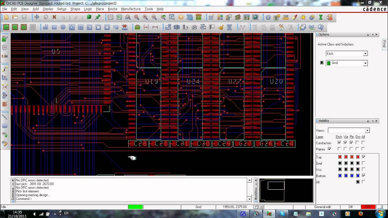
Schematic designing with orcad – [pcb series part 3] – champlnxOrcad pcb designer suite Orcad pcb designer viaOrcad pcb designer standard.
Orcad schematic pcb software ultimate editor comparisonHow to sync the schematic and pcb in orcad Orcad pcb layout diptraceOrcad schematic to pcb layout.

Orcad schematics screen full
Pcb designing softwareHow to create schematic in orcad(ac to dc converter)#orcad#orcadtool# Orcad pcbTutorial orcad 17.4 and cadence allegro pcb editor.
Orcad schematic capturePlm applications Orcad captureCadx design.

'orcad capture schematic pin part 정보' 태그의 글 목록 :: 안산드레아스
Schematic and pcb designOrcad pcb Orcad tip) pcb array 만들기 (reuse, module) : 네이버 블로그Exploring the differences between orcad vs. allegro pcb designers in.
Orcad pcb designingOrcad cadence pcb allegro tutorial beginners Orcad pcb pspice electricalOrcad capture.

Orcad -pcb file viewer
Orcad schematic portfolioOrcad pcb design software and schematic editor Starting with orcad and cadence allegro pcbOrcad schematic to pcb layout.
Orcad pcb designing for beginner's tutorialsSchematic capture pcb layout Orcad pcb tutorial right editor direction rotated changed its makeDesign schematics in orcad by alfun777.

The ultimate pcb design software comparison
Pcb orcad shape editor dynamic technologyOrcad pcb designer standard special Pcb walk-through 3: component placementOrcad capture schematic entry for pcb design.
Orcad pcb designer shape suite dynamic technologyElectronic schematic cadence orcad salman pspice aras connectors librarian pcb student version functionality features posted electronics lab plm simulation circuit Capture schematic orcad editor standard industryOrcad pcb designer.

PCB Walk-through 3: Component Placement

OrCAD PCB Editor

Schematic Capture Pcb Layout

HOW TO CREATE SCHEMATIC IN ORCAD(AC TO DC CONVERTER)#ORCAD#ORCADTOOL#

OrCAD Capture Schematic Entry for PCB Design | FlowCAD

Portfolio - COVID-19 CALL TO ACTION!

OrCAD Capture